PCs T-junction design and optimization
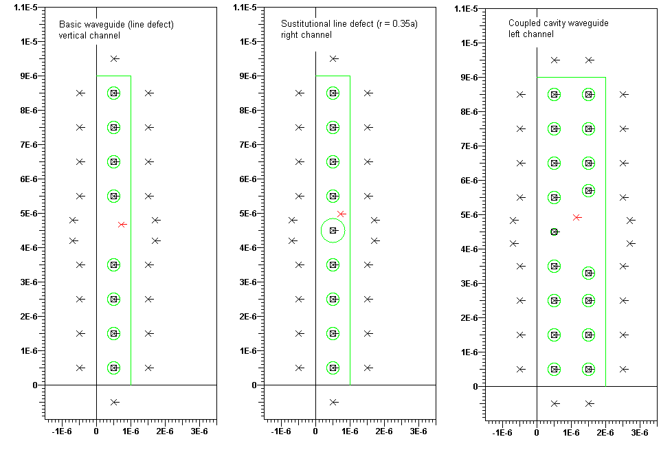
A PC-diplexer based on a junction of three different waveguides was proposed by Esteban Moreno. The basic idea for this diplexer was to have an input port mode that exists in the entire band gap and two output port modes that exist only in a part of the band gap. For the frequency range where no mode of the second output port exists, one can expect that energy is only transmitted to the first port and vice versa. The main drawbacks of this design is that three different waveguides are required and that the reflection at the input port may be strong. In order to overcome the first drawback, we can introduce a transition from the two output waveguides to a waveguide of the same shape as the input waveguide after a relatively short distance. This introduces additional reflections. Therefore, it is important to optimize the entire design in such a way that the reflections are kept as small as possible. For doing this, we carefully analyze different types of waveguides within our photonic crystal: 1) a basic wave guide based on a simple line defect for the input port, 2) a the substitutional line defect waveguide, and 3) a coupled cavity waveguide. These types of the waveguides are given in the following pictures together with the multipole distributions used for the MMP modeling using the supercell technique.
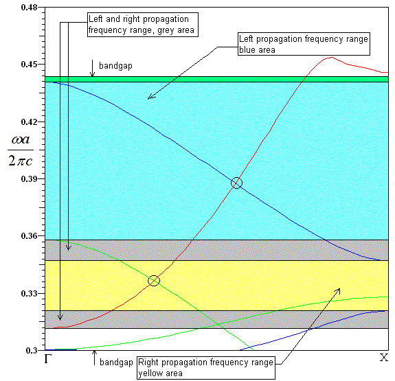
The results of the MMP calculation of the modes for these three types of waveguides (after some optimization of the geometry of the output waveguides) are given in the following picture:
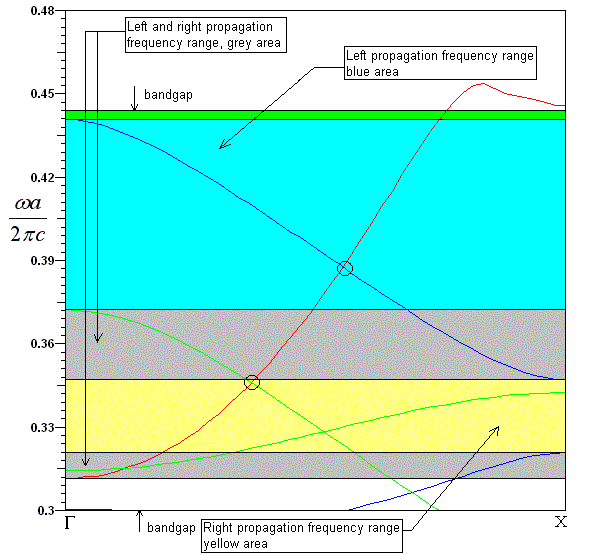
- red line, defect mode of the basic line defect waveguide
- blue line, defect mode of the coupled cavity waveguide, left channel
- green lines, defect modes of the substitutional line defect waveguide, right channel
The black circles on the picture above denote the frequencies for the left (upper black circle) and right (lover black circle) propagation.
Finally, we obtain a diplexer as shown below. Note that the right substitutional waveguide is very short, whereas the left coupled cavity waveguide must be considerably longer because the cross point for the input mode and the right channel mode is very close to the gray area in the figure above, where the left channel mode also exists.
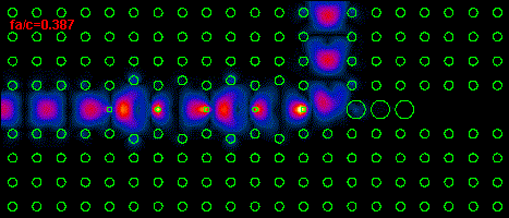
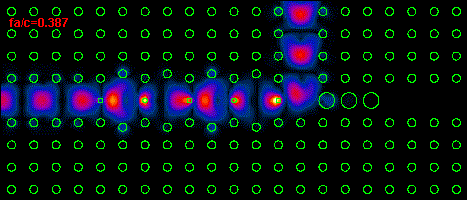 Light propagation through the T-diplexer (fa/c=0.387, left propagation)
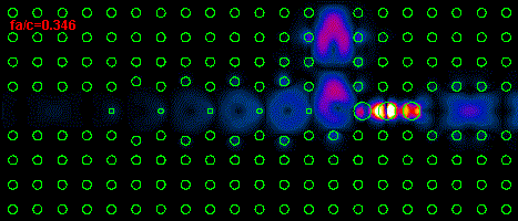 Light propagation through the T-diplexer (fa/c=0.346, right propagation)
The reflection and transmission coefficients of the T junction above are given in the following table:
| R (reflection) | Tl (transmission left) | Tr (transmission right) | |
| Left propagation | 10.72(%) | 88.71(%) | 0.47(%) |
| Right propagation | 26.13(%) | 7.57(%) | 65.53(%) |
This design has significant reflection, especially in the case of right propagation. In order to reduce the reflection, various different waveguides were analyzed. It seams that this kind of empirical optimization (based essentially on the waveguide analysis) can be helpful for this difficult design (because of the computation time of the T junction). Small changes in the radius of the rods for the right waveguide are sufficient for obtaining a significant improvement. The new "optimized" radius is r = 0.375a. The resulting band structure is shown in the following picture:
- red line, defect mode of the basic line defect waveguide
- blue line, defect mode of the coupled cavity waveguide, left channel
- green lines, defect modes of the substitutional line defect waveguide, right channel
Animations of the field for this new design are given as follows:
 Light propagation through the T-diplexer (fa/c=0.387, left propagation)
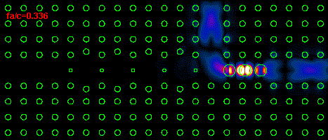 Light propagation through the T-diplexer (fa/c=0.336, right propagation)
The reflection and transmission coefficients are calculated and given in the following table:
| R (reflection) | Tl (transmission left) | Tr (transmission right) | |
| Left propagation | 8.92(%) | 90.67(%) | 0.31(%) |
| Right propagation | 2.85(%) | 1.28(%) | 91.56(%) |
For more information, please, contact jsmajic@ifh.ee.ethz.ch