PCs waveguide analysis
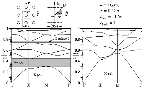
Figure
1: An example of a 2D perfect photonic crystal is
analyzed and the band structure calculation results are illustrated.
We will use this presented perfect crystal structure for making a lot of
different PCs devices. As one can see this structure
consists dielectric rods (high refractive index material) arranged in a square
lattice. The lattice constant, rods radius and permittivity
of used materials are shown.
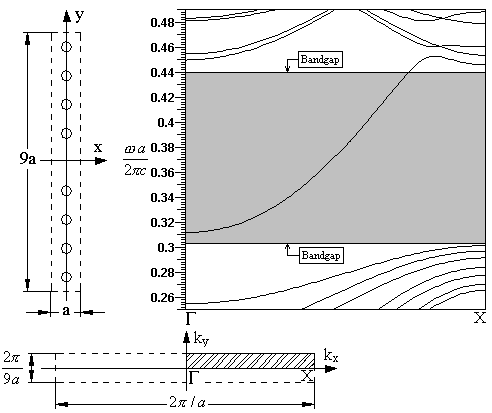
Figure
2: A simple line defect (vacancies) in our perfect crystal structure can be an
efficient waveguide. Dispersion relation
of this waveguide is given. These results are calculated using the supercell
method and MMP based eigenvalue solver.
As one can see, we have a lot of defect modes above and below the bandgap and a
single one covering an almost entire bandgap.
It means we have a single mode waveguide for the wide bandgap frequency range. The
original lattice, the reciprocal lattice and
the 1st Brillouin zone are shown, as well.
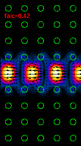
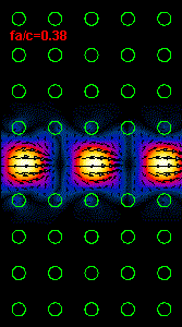
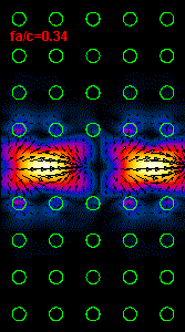
Figure
3: The infrared light propagation along the PCs waveguide at three different
frequencies (wavelengths) is presented.
Using the dispersion relation (Figure 2) it is possible to see that the left
hand side
animation belong to the upper part of bandgap,
the middle animation
is almost at the central bandgap frequency and the right animation is at the
frequency close to the lower
bandgap limit.
For the frequency range outside of bandgap our crystal supports a light
propagation and at these frequencies
our line defect waveguide
becomes useless.